I have modeled, as you mentioned, with compound. This is much better than TIE.
See the difference.
Left picture with pcb and cupper plated hole created with compound. Right with TIE constrain.
Left one running with PaStix is much more faster then the right one with Pardiso.
You may just have to adjust the position tolerance and mesh densities (same rules apply - coarser side should be the master surface) and then tie should work well. Still, it’s good when you can skip any additional constraints.
I am improving the simulation step by step. Every modification takes a lot of time.
This last simulation stopped at 90%
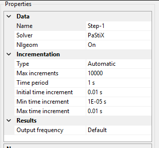
This run this on a i9 laptop with 64GB and 8 cores and this took 3331s (55min) to finish
The step setting is:
That’s why it would be good to simplify the model somehow. Maybe reduce it to the problematic contact region of the clip and pcb (especially pcb segment is too large for such local studies):
Normally, I would opt for 2D simplification, but this geometry doesn’t really match extruded (plane stress/strain) or revolved (axisymmetric) approximation.
Part of the clip too - only its small segment comes into contact with pcb when the issues start occurring. Of course, once you have a working setup, you can add the rest of the model.
In fact, you don’t even have to cut the model - you could use rigid body constraints for the irrelevant regions.
Part of the clip too - only its small segment comes into contact with pcb when the issues start occurring. Of course, once you have a working setup, you can add the rest of the model.
The clip is already simplified. All other features are removed
In fact, you don’t even have to cut the model - you could use rigid body constraints for the irrelevant regions.
Yeah, but I mean making it shorter (analyzing only the segment in contact with pcb for now).
It would be best to partition the volumes in some CAD software and then apply rigid body constraints to volumes outside of ROI, but you could use manual node set definition too:
It would be best to partition the volumes in some CAD software and then apply rigid body constraints to volumes outside of ROI, but you could use manual node set definition too:
Is it the same as making nodes outside of poi as fixed constraints?
The idea here is not to prevent the deformation of those redundant regions, but rather to significantly reduce the computational effort, thanks to how rigid body constraints work. Explanation from Abaqus documentation:
Element-level calculations are not performed for elements that are part of a rigid body. Although some computational effort is required to update the motion of the nodes of the rigid body and to assemble concentrated and distributed loads, the motion of the rigid body is determined completely by a maximum of six degrees of freedom at the reference node.
What is the objective of your simulation? Based on that you can simplify a lot your model and get results faster.
If is the insertion force, then you don’t need to do the reverse step.
If the clip is plastic and the holder is copper or other metal, then the deformation will be negligible and you can use a simple lineal material for the holder (even first order elements)
I have seen that you have modeled an intermediate part, so then you can remove the big holder part and left only that intermediate part with propper boundary conditions.
You can model in CAD that intermediate part as a surface and create a shell mesh + mesh extrusion for getting a one element thickness model mesh with hexa elements, the best for contact, and again you will reduce the node count a lot.
If you need the maximun stress in the clip part during the insertion process, then you don´t need to model the contact or holder at all, just apply a radial displacement on the clip faces, or include the holder and apply a radial deformation on the holder to get the worst deformation/stress of the clip.
To replace soldering connectors on a PCB, a press-in feature is replacing the classical solder post on the connectors. This feature will be pressed in a copper-plated hole.
The press-in feature must deform plastically to have the best contact force. When pressed in, a certain retention is needed.
The press-in force gives, during assembly, good feedback on the quality of the connection.
The copper in the PCB hole is very ductile, with large elongation at break.
The simulation is to see what the forces and the deformation of the parts will be. The simulation will be done on nominal dimensions, dimensions with maximum interference, and dimensions with minimum interference. The press-in features will also be tested with samples to validate it.
It is the best I can get. Higher K factor will not converge .
The difficulty is to find the right K factor to get also good results and good penetration.
I have done a simulation with a range of K factors according to the specification I found in manuals and forum. K=5 to 50 times Young Modulus and Young Modulus divided by the adjacent cell length.
I’ve not read all posts (i don’t think it has ever been evoked), but, as an open discussion, regarding the dimensions of the parts, i’m wondering if the micron units system would not be more relevant (to limit round error - source of convergence difficulties?):
as you know and properly speaking, you must be units consistent when using a solver such as Calculix
in attachment, i’m sharing the units a used in the past to work a electronic chips
I would try Half model not 1/4 to avoid mixing contacts and BC.
No friction and no tangential stiffnes untill you solve the penetration issue.(use 1st dummy step)
I would like to help some more but your model is a minimum of 1h each run and it was missing a main component from the beggining.
NOTE: Request the history output for the overal reaction force at the symmetry plane of pineye. It can be usefull later to get some idea of the Friction force involved.
By other hand, sorry if my comment is obvious but, (its just in case), check if you should compare your result or your result x 4 against the reference value.
That’s why it may actually be good to vary it exponentially.
Interesting idea and it can make sense for tiny components, but it’s quite risky in terms of getting all inputs right (especially the non-standard ones such as contact stiffness) and interpreting all outputs correctly.